7 Crucial Steps How to Create the Ideal Semiconductor for Large Language Models
In the fast-evolving world of artificial intelligence (AI) and semiconductor technology, large language models (LLMs) are at the forefront of technological innovation. These models, which power everything from sophisticated chatbots to complex data analysis tools, require advanced semiconductors that can handle their immense computational demands.
To meet these demands, the semiconductor industry is working on designing specialized chips that can handle the specific needs of LLMs. In this blog post, we’ll explore how to create the ideal semiconductor for advanced language models, focusing on key considerations in design, fabrication, and optimization.
Understanding Computational Demands of LLMs
Before diving into chip design, it’s crucial to understand the computational demands of LLMs. These models rely on massive datasets and complex algorithms that require substantial processing power. Key characteristics of LLMs include:
Designing Chip Architecture for LLMs
Creating a semiconductor for Large Language Models (LLMs) begins with designing an architecture that meets the specific needs of these models. Key architectural considerations include:
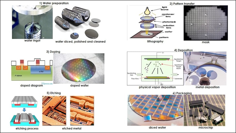
Fabrication Process
Once the chip architecture is designed, the next step is fabrication. This process involves creating the physical chip using advanced manufacturing technologies. Key factors include:
Optimizing Performance and Energy Efficiency
To build an ideal semiconductor for LLMs, optimizing for both performance and energy efficiency is essential. Strategies include: Intel Announces Two-Year Warranty Extension on 13th- and 14th-Gen Core Processors – techovedas
Validation and Testing
Before a semiconductor can be released to the market, it must undergo rigorous validation and testing. This process includes: Apple New Heartbeat-Based Authentication: A Revolution in Biometric Security – techovedas

Market Adoption Strategies
Once the chip is validated, the next challenge is market adoption. Strategies for successful integration include: A Platform to Practice Digital Design & Immediate Feedback: HDLBits – techovedas
Future-Proofing and Innovation
To ensure the semiconductor remains relevant as technology evolves, consider the following: SK hynix Unveils LPDDR5T RAM: 13% Faster Than LPDDR5X – techovedas
Creating the ideal semiconductor for advanced language models involves a multifaceted approach, from understanding Large Language Models (LLMs) requirements to designing, fabricating, and optimizing the chip. By focusing on custom architecture, efficient manufacturing, and performance optimization, semiconductor designers can build chips that meet the demanding needs of modern AI applications. Additionally, addressing market adoption, future-proofing, and ongoing innovation will be key to maintaining a competitive edge. As the field of AI continues to evolve, the advancements in semiconductor technology will play a crucial role in shaping the future of artificial intelligence.